
Perovskite Cell Sputtering Equipment
Classification:
Designed for university and research institute laboratories for the preparation and study of various materials, including metals, semiconductors, nanotechnology, and insulators.
Contact:
Details Introduction
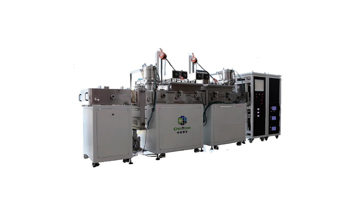
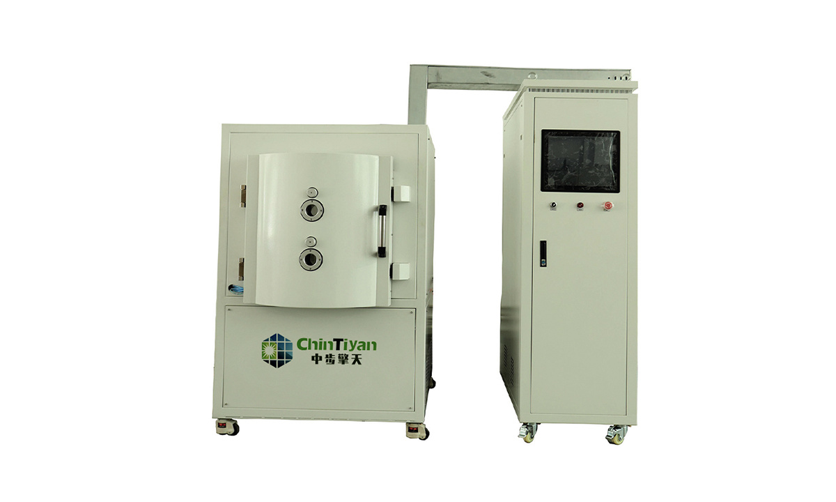
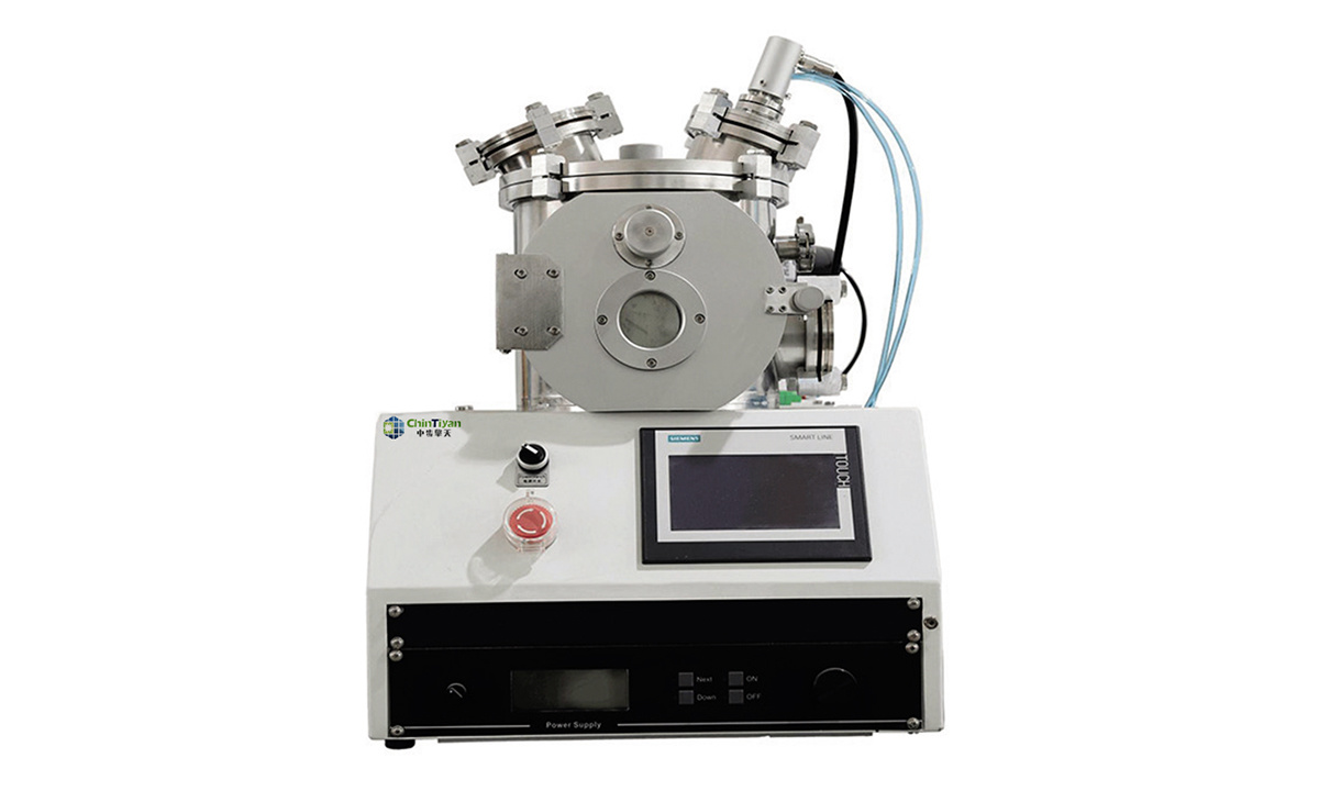
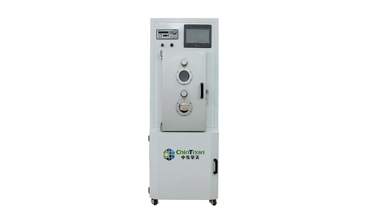
PD-500c/600c magnetron sputtering equipment is designed for university and research institute laboratories for the preparation and study of various materials, including metals, semiconductors, nanotechnology, and insulators.
1.Siemens PLC + touch screen for manual/automatic control, or fully automatic computer control.
2.Equipped with four 2–4 inch magnetron sputtering targets, capable of sputtering on 2–8 inch wafers; uniformity within an 8-inch tray is better than ±3%~±5%.
3.Optional sample loading function available.
Parameter
|
Chamber Dimensions(304 stainless steel) (L x W x Hmm) |
500×500×500mm/600x600x500mm |
| Ultimate Vacuum | ≤5.0×10⁻⁵ Pa |
| Pumping Speed | From atmosphere to 8×10⁻⁴ Pa≤30 min |
| Substrate Holder | Max. heating temperature: 500-800℃ |
| Sputtering Size |
Up to 8-inch wafers;Supports 4-inch, 2-inch, Φ45mm, Φ30mm;Small square substrates Rotation speed: 0-30 rpm (continuously adjustable) |
Description



Production Strength


Can This Laminator Adapt to Your Existing Production Line and Different PV Module Types?
The solar panel laminator offers strong compatibility – it handles conventional, glass‑glass, flexible, high‑efficiency, and shingled modules. We provide multiple configurations (single/double‑layer, dual/triple‑chamber) and flexible platen sizes to match your space and capacity. Its automated material handling seamlessly integrates with upstream/downstream equipment, supporting continuous high‑throughput production with ≥99% uptime to meet your output goals.
How Does the Solar Panel Laminator Ensure Module Quality and Prevent Bubbles or Cell Breakage?
The solar panel laminator uses a triple‑chamber design (preheating + lamination + curing) with independent temperature and pressure control for each stage, precisely matching the EVA cross‑linking process. Combined with a high‑accuracy vacuum system, this effectively eliminates bubbles. The fully automated infeed/outfeed reduces manual handling errors, significantly lowering breakage rates and ensuring high yield and long‑term module reliability.
What Defects Are Common In Perovskite Module Manufacturing?
Common defects include pinholes, uneven crystallization, interlayer delamination, and edge sealing leakage. These issues are mainly caused by process instability and environmental exposure, and are reduced through controlled coating systems, vacuum environments, and precise edge sealing processes.
What Are The Main Challenges In Perovskite Module Production Lines?
Key challenges include film uniformity control, moisture sensitivity, and large-area coating consistency. Small process variations can affect crystallization quality and module efficiency, making precise process control and environmental stability essential for mass production.
Contact us
Address: 5 Xingfu Road, Miaoshan Development Zone, Jiangxia District, Wuhan City, Hubei Province, China
Scan QR Code by WhatsApp